Early Designs: Wireless Retrofit for NES and SNES controllers
2014-12-07 19:46 - Making
I learned about a fancy chip called the nRF24L01 a while back. It packages up all the hard work involved in wireless data transmission into one simple chip. And it's available online for quite cheap. I've also got a great collection of video game consoles. Most of them either came with wireless controllers by default, or it's easy to find aftermarket controllers that add wireless support. Not so for the original Nintendo console. Which set me down a bit of a path.
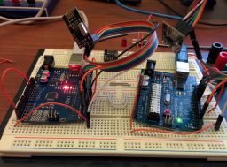
 I got some of those chips and hooked them up. Actually, I got what turned out to be some cheap knockoffs, which didn't work, first. But the second set I tried (ten for $5!) worked great. They were only sitting a couple inches apart, but I could reliably send data from one to the other, and observe the acknowledgement sent in reply. Overall, that was the easy part. I have to decide exactly how to read which buttons are pressed, plus when and how to transmit that data wirelessly to the receiver half, but there's plenty of good options to choose from, and software is easy to fix. What I really want is a good wireless controller that will work for the original NES. One for the Super Nintendo wouldn't be bad either. Turns out the controllers are almost identical (besides of course the extra buttons), so if I want I can make one SNES controller that will work (with the right receiver) on either console. So that's my goal.


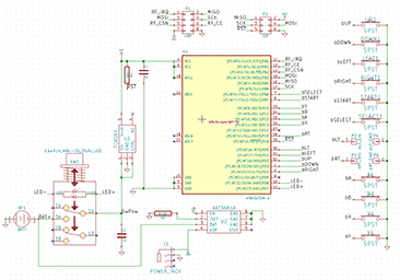
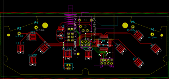
This weekend I've been working on the more complicated bit: the circuit. I've used Eagle once before. I put a few hours into the schematic before I tried to turn it into a PCB layout and realized that I want to make something about 13x5 centimeters, but the free version of that paid program is limited to 10x8. Too small! So this time I tried KiCad a similar, but open source and thus not limited, program. The picture above left is the schematic. The giant yellow box is the Atmel ATMega328 micro controller, above it two connectors (one for the nRF chip, the other a programming header), to the right all the buttons of the controller, and the rest is the power circuitry including an illuminated pushbutton switch to control power and display status. On the right is the PCB holding all of those. Credits to Andy Goetz who did the hard work of getting the outside cut edge to lay out the correct way for a very similar project. (Though I had to post-process his work a bit to import it, plus that's his most recent post and it's over two years old, so I wonder if he finished?)
I've still got a ton of work ahead. I want to be really sure that all this is right before I send it out to be made. It will cost in the range of $50 to make the PCBs, which I don't want to waste. Not to mention triple checking that all the parts really fit where I've put them, I especially need to double check the battery charging circuitry. Don't want to blow up a battery and ruin all this hard work!