Nevo C2 Remote Control - Reverse Engineering - Part 1
2016-03-07 19:36 - Making
I've been a fan of JP1 Remotes for quite some time. There's a wonderful community that has written software to put the user in total control of all the features they make possible, and even written "extender" software to add additional features. My approach for some time has meant turning on all the right devices (player, TV, receiver) and set them all to the right inputs, at the press of one button. Then turn them all off with the press of another.
Most recently I've switched to the "Nevo C2" remotes (also known as "Xsight Color" or "ARRX15G"), which have a graphical display built in. This makes it easy for me to deal with the huge array (TiVo, HTPC, plus eleven game consoles) of devices I've got hooked up. The built in software is pretty good, especially with RemoteMaster to customize it. But it's pretty clunky in some areas. At one point I found a post with pictures of the inside of my remote. The post was meant to highlight the (very minor) differences between two similar models. In the full size image, one can just make out a big ARM chip in the middle. I got interested in discovering more about the innards of these things, and how hackable they could be with some reverse engineering. So I ordered an extra one to take apart and tinker with, with no worry of damage. (They can be found on eBay for around $16, so this isn't a huge investment.)
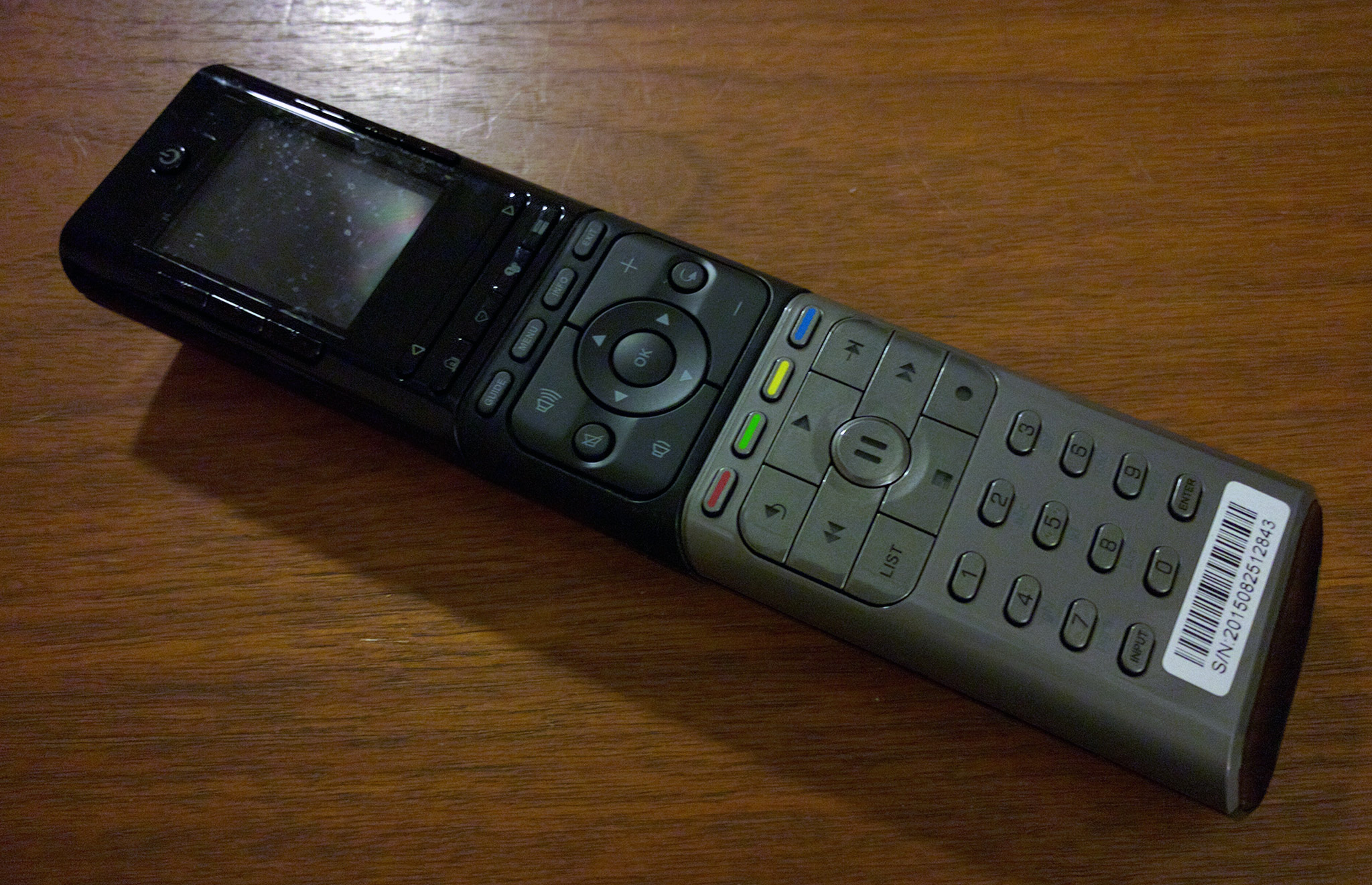
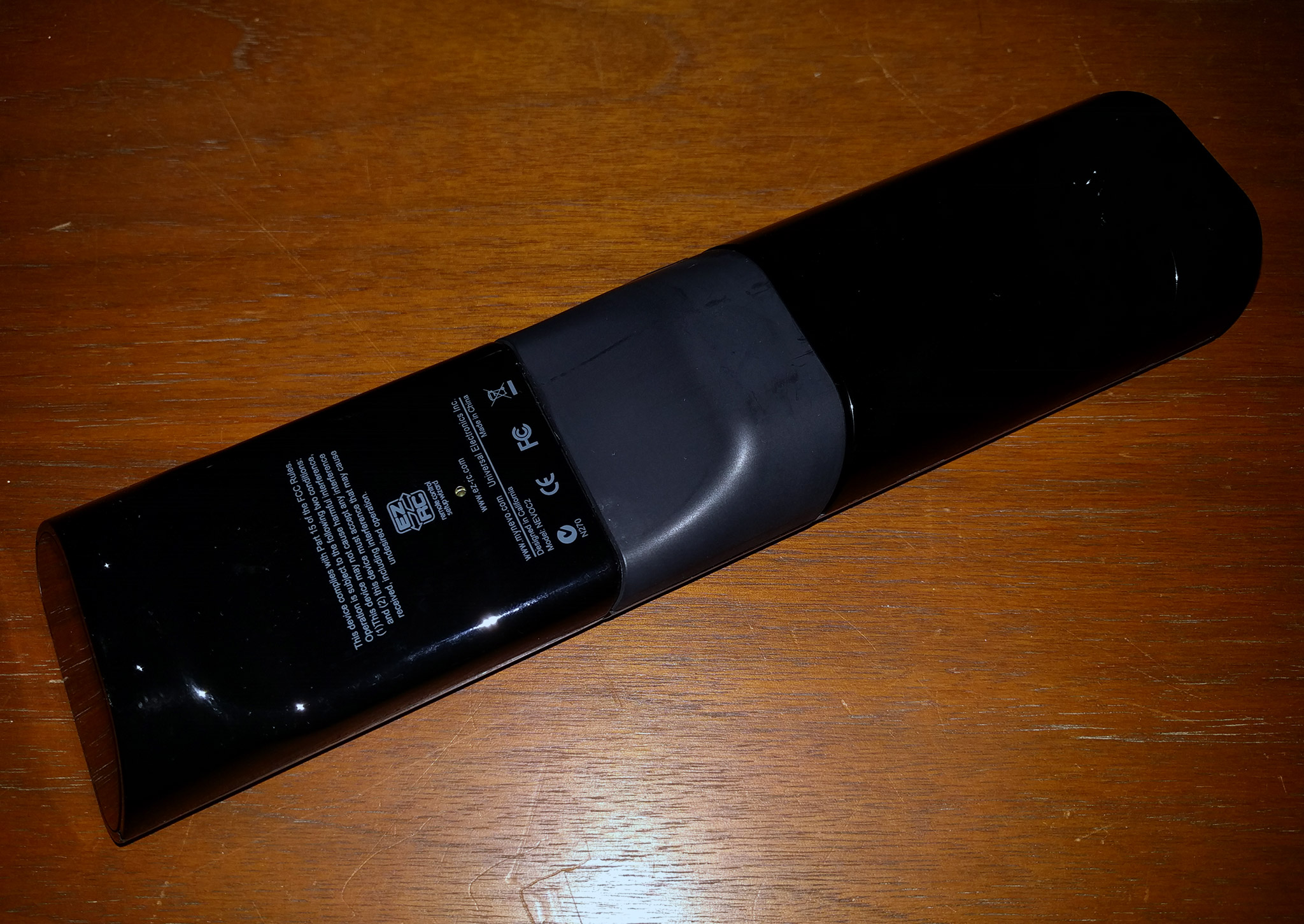
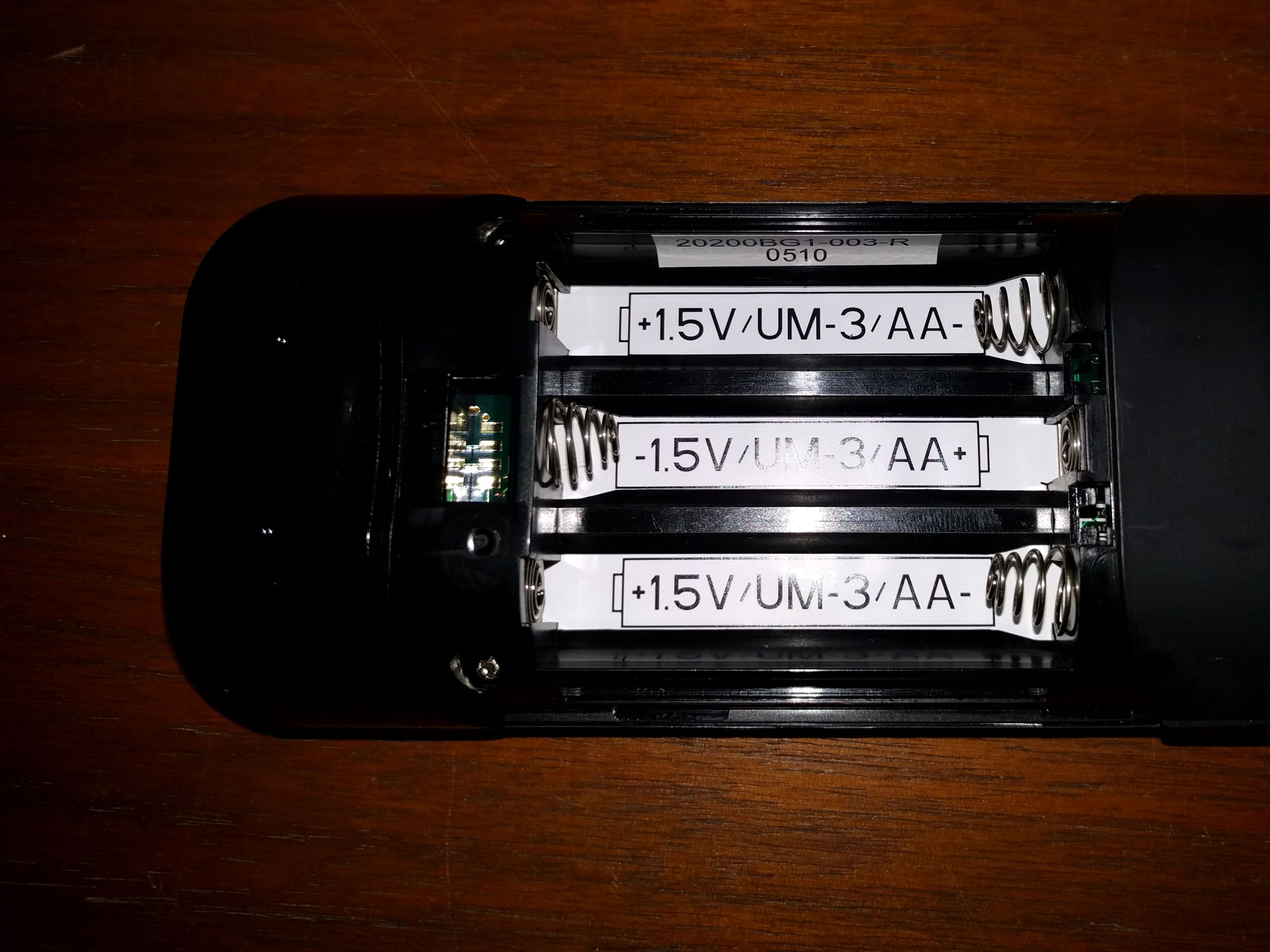
Just for posterity, here's the external view of the remote. Front, back, and battery compartment. Forgive the crappy shots, this isn't the interesting bit. Except the battery compartment, which shows eight exposed pads which are fully accessible, at the bottom of a rather deep/narrow opening. What exactly they're for is very much worth looking into. But what I really want to do is highlight the insides. It's a good thing I bought a sacrificial unit to do this with. I cracked about half of the clips off to get the thing open. Brittle plastic, plus I didn't know the layout. I also ended up ripping the leads right off of the piezo buzzer once the two halves finally separated.
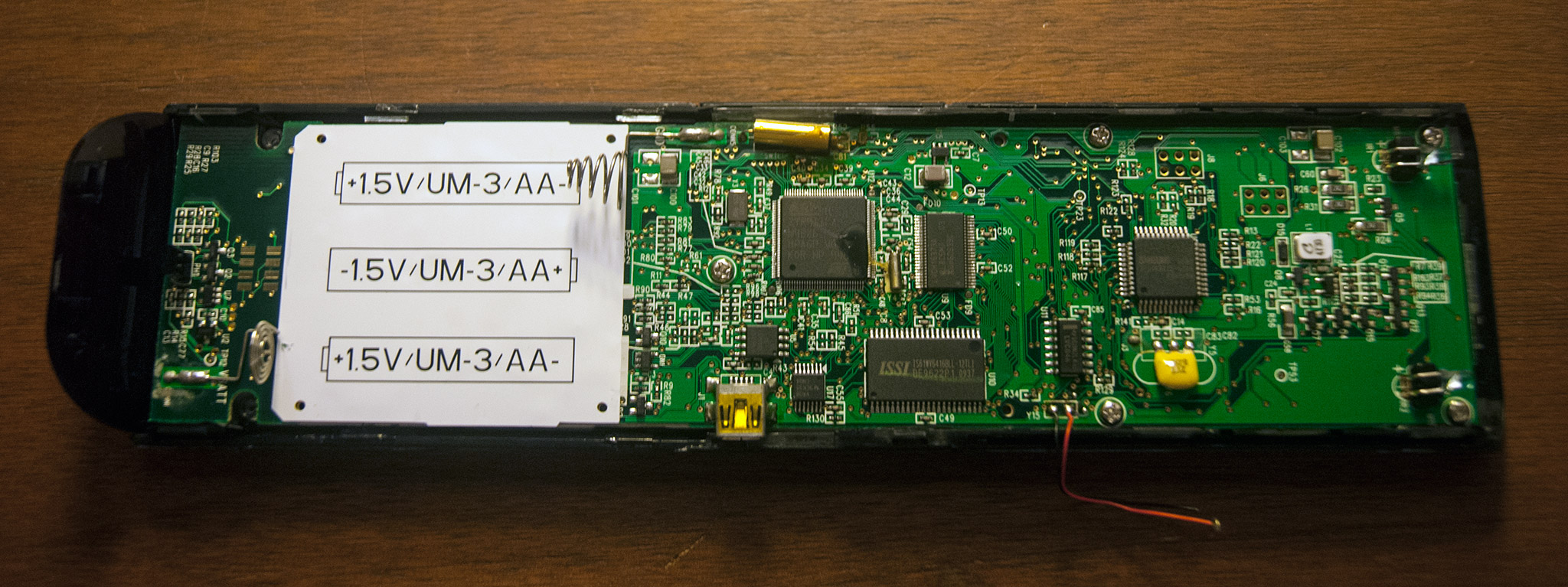
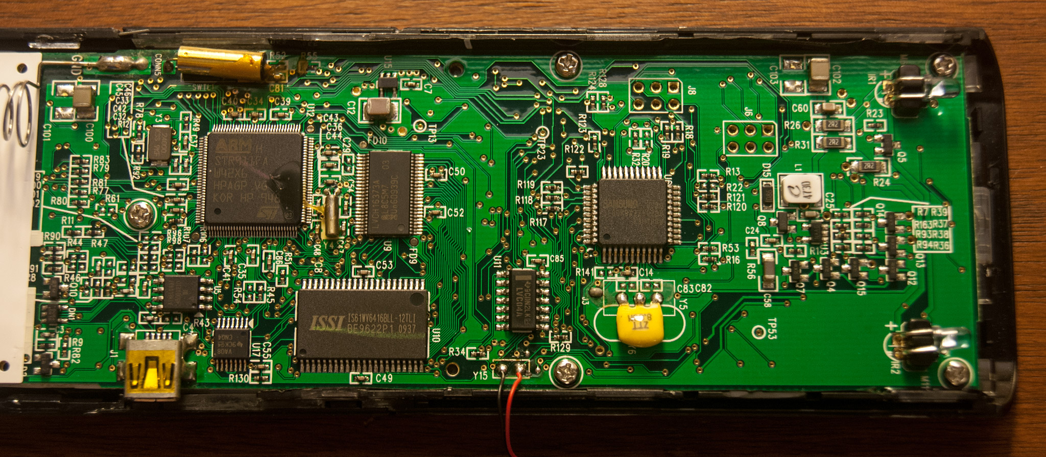
First, here's a full shot of the immediately accessible (once opened) side of the PCB. The battery compartment is towards the left. On the far left are the previously mentioned exposed pads, plus a little circuitry which at first glance seems to be only related to the photodiode located there for learning capabilities.
The interesting bits are all at the other side, the right in this image. That area has been separately shot in a more close up view. I'm going to concentrate today on identifying the chips, so here's another copy of that image, with numbers overlaid for reference in the following commentary.
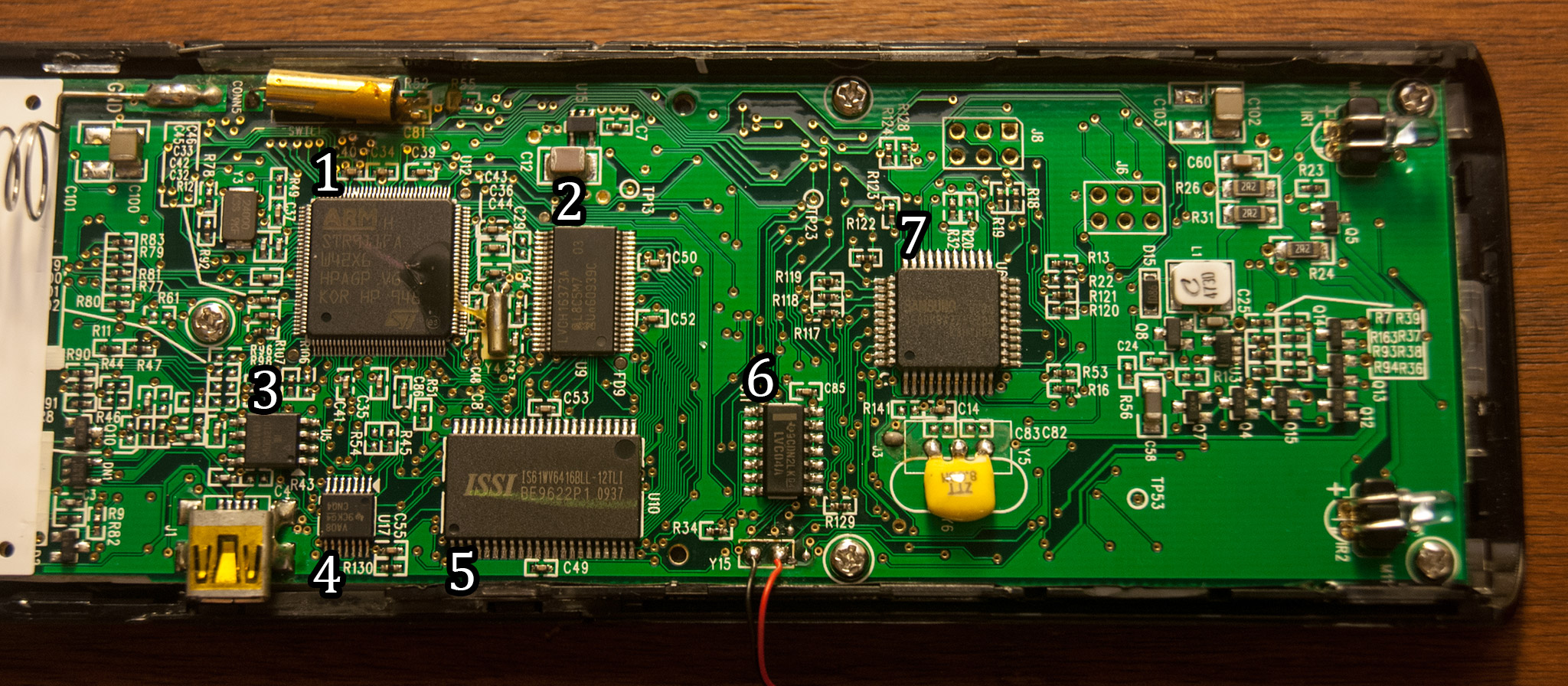
I've called out seven chips that seem especially interesting.
Chip 1
There's a large ARM logo at the top (with an "H" next to it), and STMicroelectronics logo at the bottom. The rest of the text reads:
STR911FA
W42X6
HPAGP VG
KOR HP 948
This has got to be a STR911FAW42 chip which confirms that it's a 32 bit ARM MCU. The datasheet tells us that the 911FAW42 has 256+32 kB of flash and 92 kB of RAM, and comes in a LQFP128, which all seems right. Finding the programming pins, and ideally some spots that are more accessible than the tight pitch pints themselves, will be interesting.
Chip 2
This chip has no obvious (to me) markings besides the NXP logo which is upside down in this image. The text on it is:
LVCH16373A
L8C5M7      03
UnG0939C
This turns out to be a simple 74 series 74LVC(H)16373A: 16-bit D-type transparent latch with 5 V tolerant inputs/outputs; 3-state. A latch/flip flop. Curious.
Chip 3
This tiny chip is unreadable in the images so the text transcription will be extra important. By the look of it, an eight pin SOP, I'm guessing serial flash.
ATMEL0937
45DB321D
    SU
First, I see the second apparent date code: this 37th, chip 2 38th, week of 2009. As far as I know these remotes are discontinued, so it looks like I've gotten some "new old stock" here, which might help explain how cheap they are. Either way, this definitely looks like the 32Mb, 2.5V or 2.7V Atmel DataFlash (Update: I had the wrong link, for part B not D here originally; Atmel doesn't have the D part on their site?!) by the part number on the second line. The remote supports adding custom icons, so the bulk storage in addition to the flash built into the MCU makes sense. This is the second part I'll be very interested to try to dump. It's probably wired straight to the MCU, but it's a much wider pitch part; I can solder breakout wires by hand without much fuss.
Chip 4
This chip is also small, and upside down in the image. A TI logo is visible. Its text is:
VA08
9CKG4
CNQ4
This turns out to be a SN74ALVC08 QUADRUPLE 2-INPUT POSITIVE-AND GATE, and the data sheet tells us that the top marking is indeed "VA08". The package lines up as well, so I have no reason to doubt this yet. The amount of glue logic is a bit surprising, though.
Chip 5
I've used an ISSI memory chip myself before, so I think I know what I'll find just by seeing the logo. But for completeness:
IS61WV6416BLL-12TLI
BE9622P1 0937
Yet another date code confirmation, this device is from late 2009 for sure. As suspected, this is a 64K x 16 HIGH-SPEED CMOS STATIC RAM, 1 megabit of RAM addressable as 16 bit words. I can probably ignore this chip. If I can dump and restore the firmware, I probably won't need to examine the expansion RAM. The bulk flash made sense, but I'm especially surprised to find a separate RAM chip on the board. I wonder what in the design necessitated this, that the RAM built into the MCU was insufficient?
Chip 6
I can see from a mile away that this is another standard series glue logic chip. The TI logo is visible in the corner, and the text:
9CDN2LKG4
LVC04A
We only need the second line to see this is a SN74LVC04A Hex Inverter. Nothing to say about that until I trace out where the connections are going. Physically it's between Chip 6 (RAM) and ...
Chip 7
This one's interesting! With my naked eye I can really only make out the bold Samsung mark. I need good lighting and magnification to make out the text:
U930
3F80KBXZZ-QZ8B
K3HTHRN
This is as best as I can tell a S3F80KB 8-BIT CMOS MICROCONTROLLER, a secondary MCU‽ The plot thickens. Traces definitely must be found. What does this connect to, vs. the ARM MCU? Thankfully not terribly fine pitch, so again something I can work with. This is located towards the top, near the screen, is it related to that? There's also an obvious 8MHz resonator right next to it. Now I know why; I was surprised to see it before, when I saw what clearly seemed to be an SMD 24MHz crystal next to the main ARM MCU.
Interesting Bits
Near chip 7 are J8 and J6, two unpopulated 2x3 0.1" connectors. Near chip 1 is a metal tube, this is a tilt ball switch; the remote will (optionally) light up its display when moved.
Next Steps
I've got lots of things to do. An extra reason I wanted to order an extra remote to hack on is the firmware. All the ones I actively use are already in use, and I had to upgrade the firmware to be able to use them. I'm hoping to dump any contents of any flash memory on the device before ever plugging it in for real. There's a (mini) USB connector on the device (J1, near the bottom left of the close up view) for hooking up to a computer. I'd like to be able to compare the pre/post upgrade contents of the raw flash, plus make sure to monitor and log every possible (network, USB) interaction when upgrading the device. If I manage to do anything useful, it will almost definitely mean putting an alternate firmware together.
Figuring out where J6 and J8 go may prove enlightening/useful. Also the unlabeled exposed pads down by the batteries. There can't be much under the battery sticker, but some silkscreen markings are half covered at the edges, so perhaps something. Examining the other side of the board may be important as well, but these are tasks for another day!
2016-05-03 00:08 - impeeza
Hello I want to thank you for all this hard work on this project