nesRF
2015-02-22 15:23 - Making
I've been working since Thanksgiving on my nesRF project, which I've posted about several times already. The point is to retrofit the innards of a real original Nintendo controller to support wireless communications, functioning with a real console. The long story short is that I'm very close to having the project done. Well, the first phase at least. Here's all the juicy details of the whole thing, as one nice self contained post which serves as a nice summary. Of what went well, and what went less well. It runs roughly in chronological order over the things I actually did, and is chock full of pretty pictures.


First here is some physical layout. This is one of the things I was most worried about. It's worth noting that there are plenty of similar projects already online. They generally aren't pretty outside, and occasionally downright ugly inside. I wanted mine to both look and work great, but I have limited "machining" capabilities. I specifically selected a latching push button to control power, with a round button cap (so all I have to do is drill a round hole), with integrated dual-color LED for status indication.
These pictures show me first planning and then the result of drilling the hole for this push button. Note the tiny divot visible in the first picture. It was simply placed with a utility knife, then I progressively drilled smaller-to-larger holes guided first by that divot and then by each previous hole. It worked mostly perfect. The final hole was clean and round and fit the button perfectly. Except, it was in the wrong spot. My best attempt to measure the position was not good enough, it was too high, so I had to expand the hole a bit. This was operating on the one spare controller shell I had, so I thought it was OK: I learned to be careful on the real one. Somehow on the first real controller I made almost exactly the same mistake. So my hole isn't terribly pretty. Since things didn't line up perfectly first time, I had to expand the hole even further to really get proper clearance enough to allow the button to push in and out.


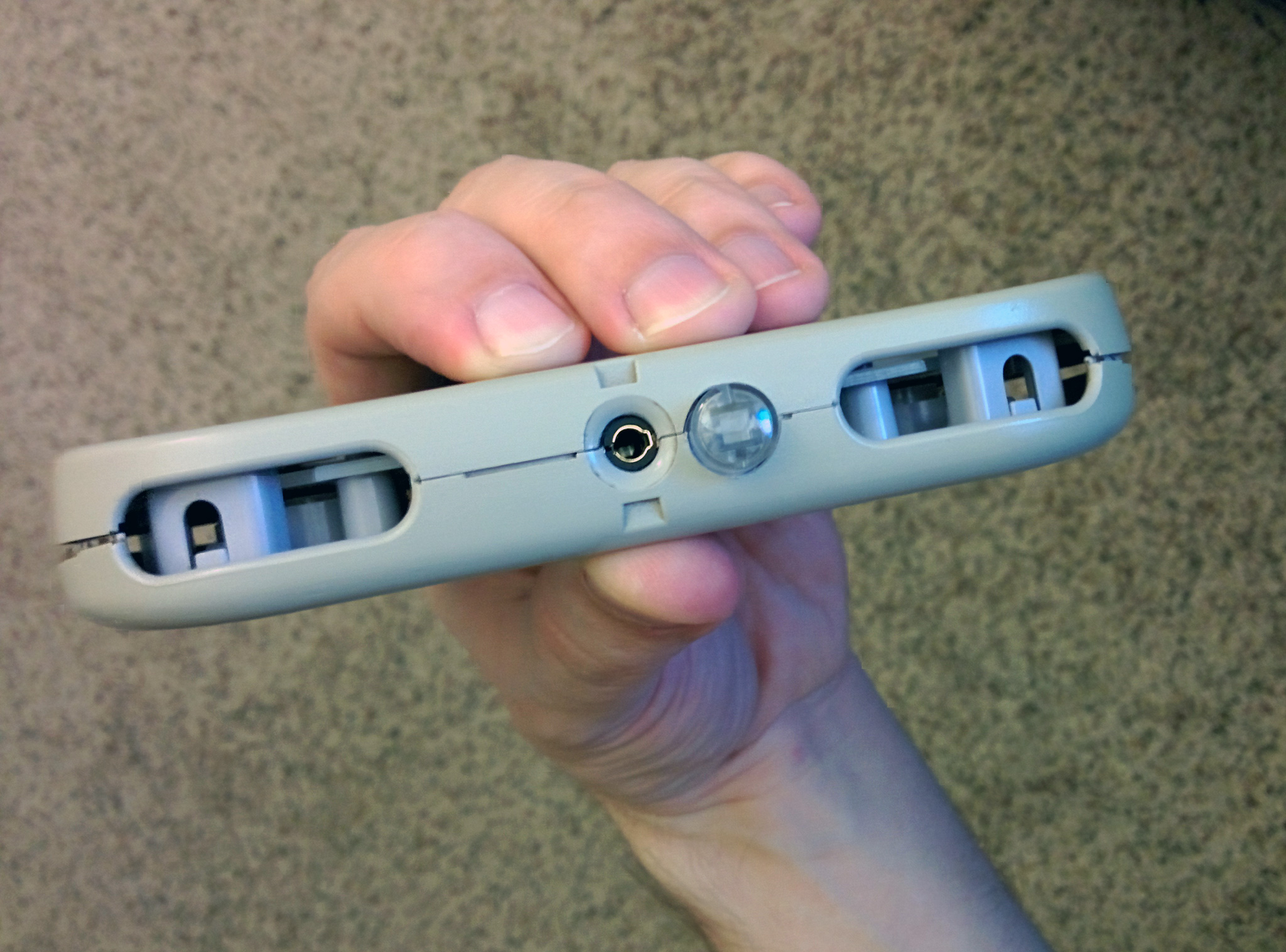
Next, the internals and the connector. Several plastic supports inside the case exist to route the cable where it needs to go, and absorb any strain of pulling on the cable. My plan is to remove the wire and put new components in that space, so they have to go. If you look carefully you can see the slightly rough edges where I've cut various bits out of the plastic case. Almost all the removed material is just inside the original cable hole, on both the top and bottom sides.
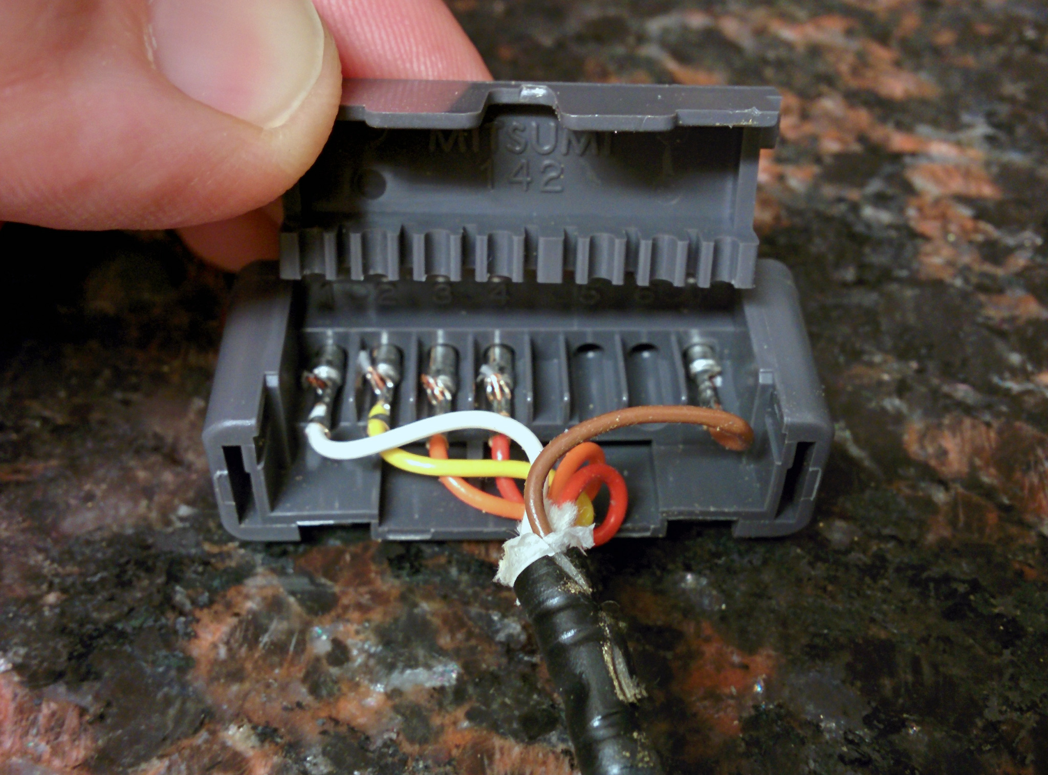

Next up is the connector end of the controller. My plan is to fit the entire receiver circuit inside this connector. The first step is opening up the connector and freeing the individual wires of their strain relief device. Opening the connector is quite difficult, I managed to design and 3D print a tiny jig to press in both of the catches on a side at once which helped tremendously. Then there's lots of plastic to remove, to make room. The original connector has a large hinged assembly, which fits around the metal connector pins to hold them in place. I used a dremel to cut off that hinged assembly, and plenty of the extra plastic bits besides. Then super glued the pins back into place.
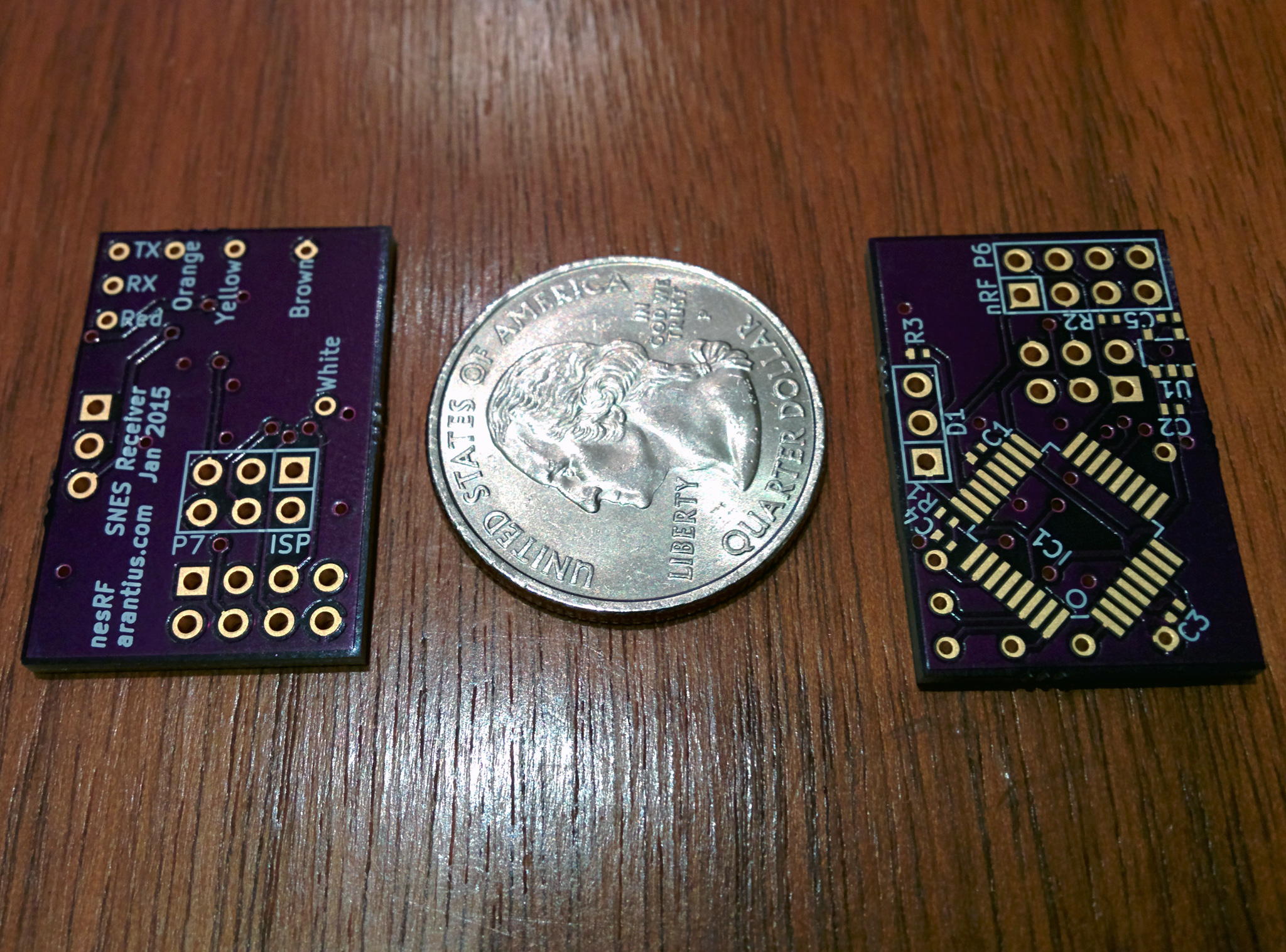
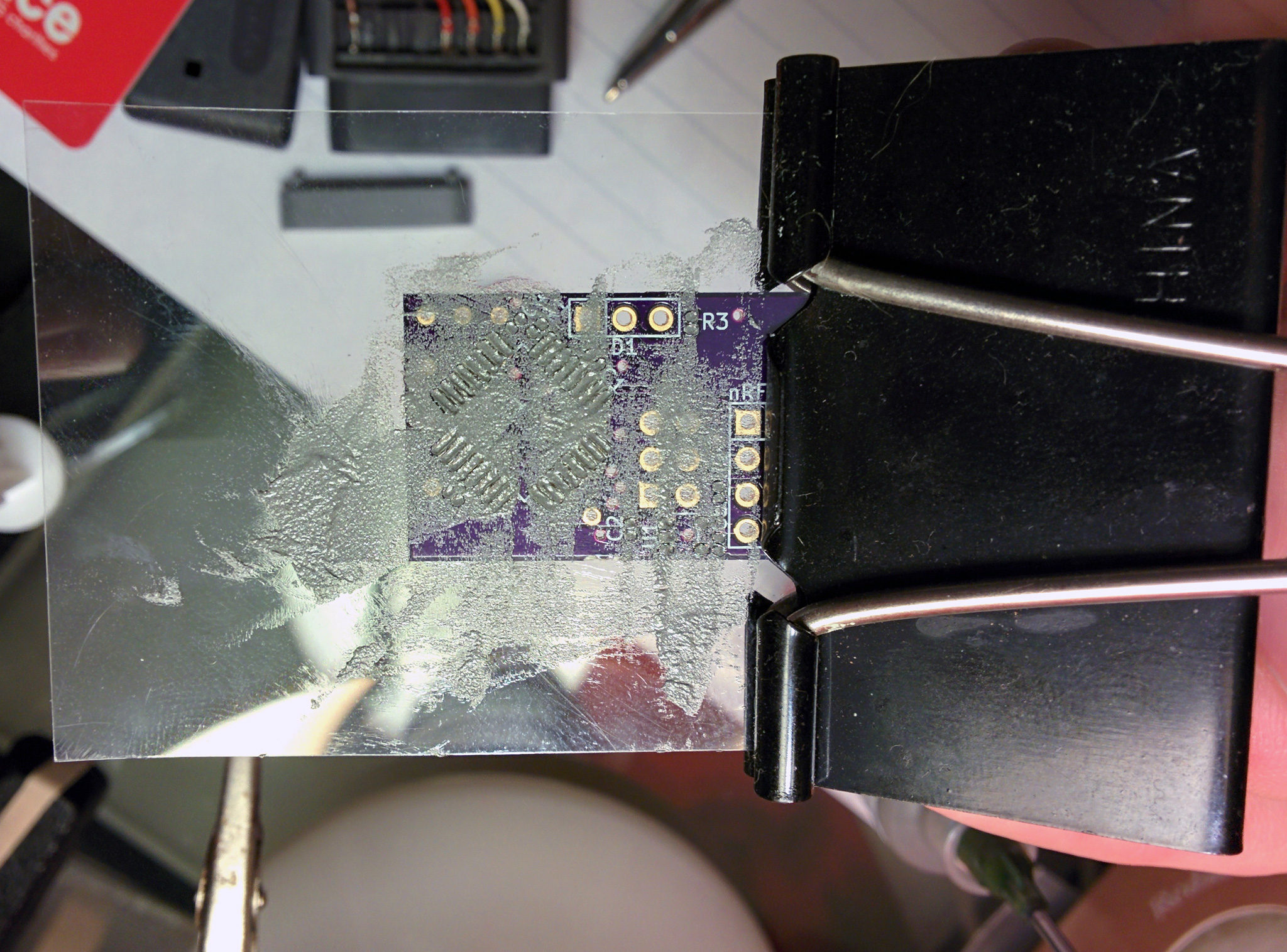
Fitting the receiver circuit into the small connector was a challenge. It was one of my main goals however, as it will look much nicer than anything else I could build myself. So all the electronic parts are surface mount varieties. These are much smaller than the alternative, which I need. But it makes working with them extra difficult. I'm lucky enough to have access to a laser cutter, which I used to create a stencil. The stencil is used with solder paste, which is a set of microscopic balls of metallic solder mixed with a paste of other active and inert ingredients not completely unlike toothpaste. With the solder paste spread over the stencil, it sticks to the circuit board in just the right places. This is the first time I've ever worked with surface mount parts or solder paste so I was operating mostly in the dark. The solder paste result looked pretty good to me, but I was concerned about how much paste was left for the pins around the microcontroller.
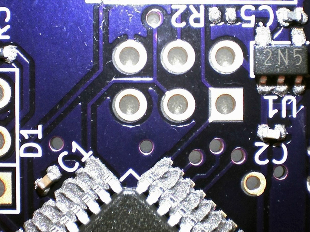
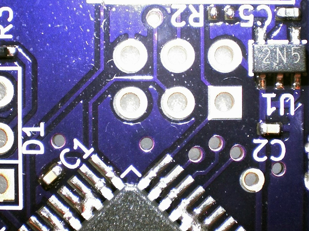
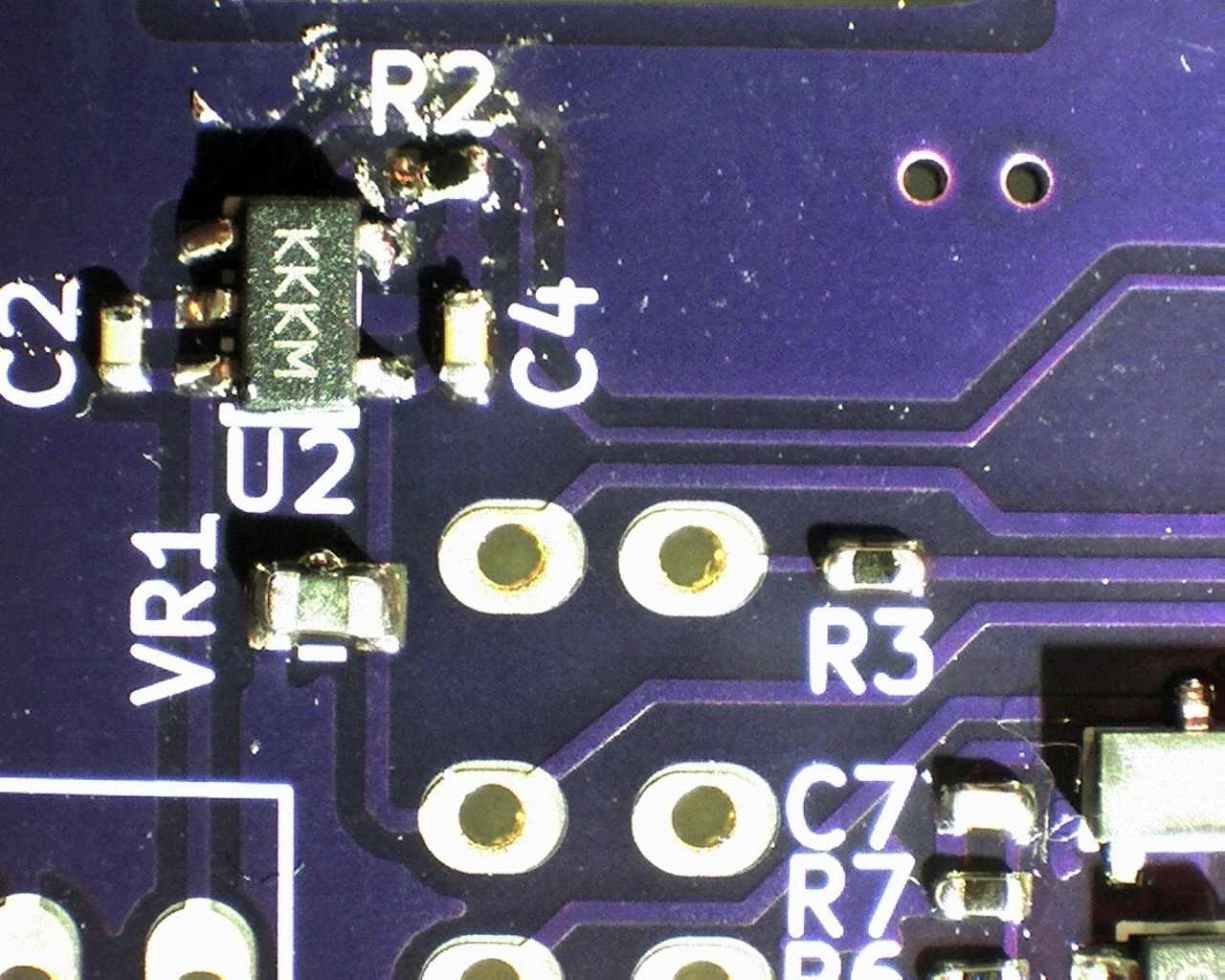
Here's a pair of microscope shots. Only ten times magnification, but it reveals quite a lot of detail. On the left is the board assembled with the paste. The solder paste is just sticky enough that you only need to touch the components into the right spot and they stick in place. With that done (all my parts go on one side) it's time to melt the solder and permanently attach the parts. I used the "hot plate" technique. Actually with an old skillet (now clearly marked "NO FOOD" due to my use of leaded solder) on the stove. I mostly just set it to medium heat and waited. The inert ingredients (I'm thinking the petroleum jelly) in the paste started to melt rather quickly. It took a few minutes and then shiny molten solder began to appear. The second shot is after everything cooled down. The small components all stuck wonderfully. As I feared, the pins on the microcontroller were bridged. There was so much excess solder that it ended up climbing the legs (capillary action) and leaving blobs of solder connecting various pins. Some careful work with solder braid sucked out the excess.
It's also worth looking very carefully at the two pictures and comparing them. Especially note the position of C2. When the solder melts into a liquid, it has a surface tension just like water. This tension will actually act to pull the components into the proper place! The solder mask (the purple stuff on this board) repels the molten solder, but the solder sticks to the exposed metal pads as well as the components, lining them up with each other like magic! This makes assembling tiny surface mount parts by hand more practical.
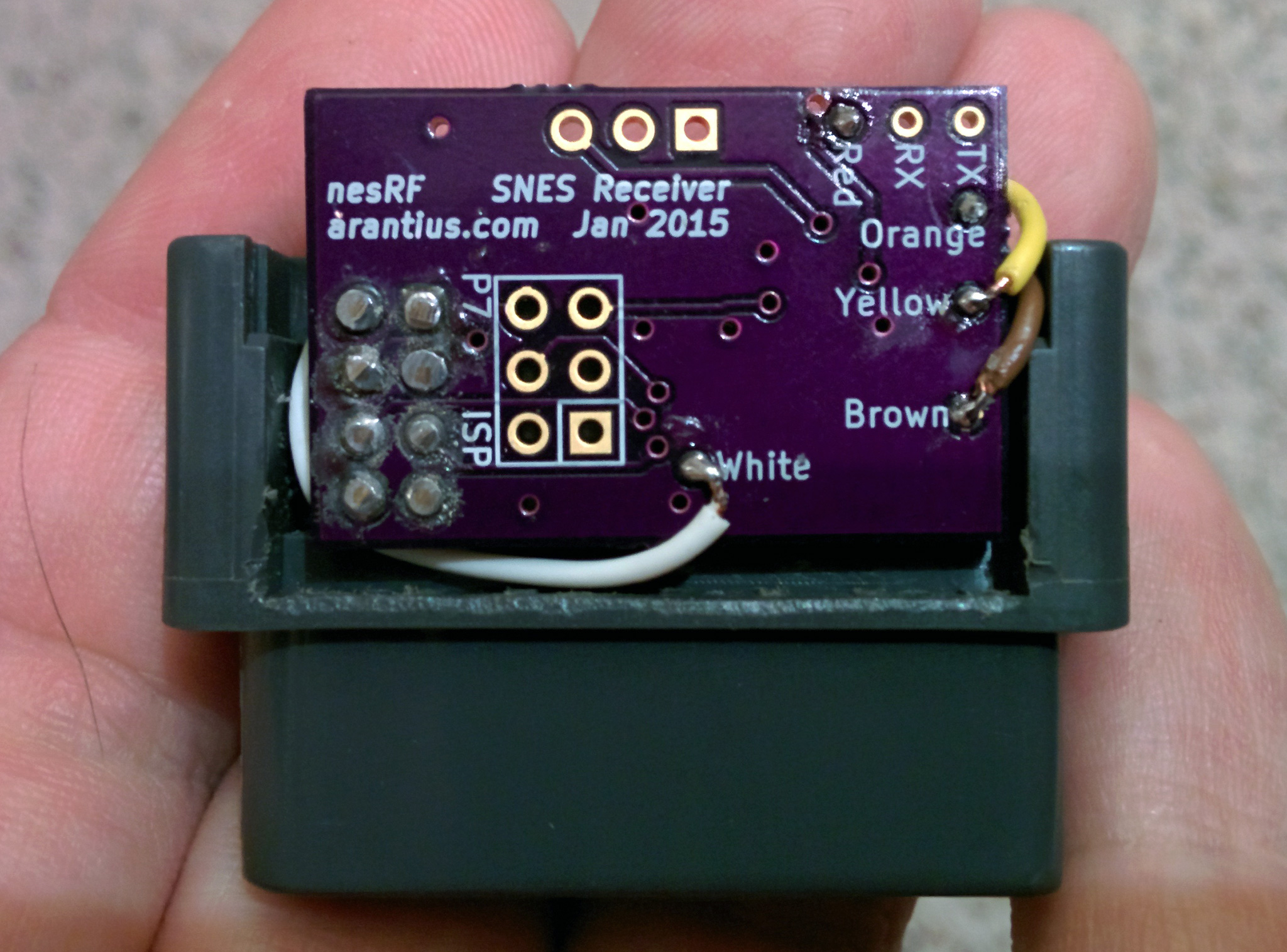
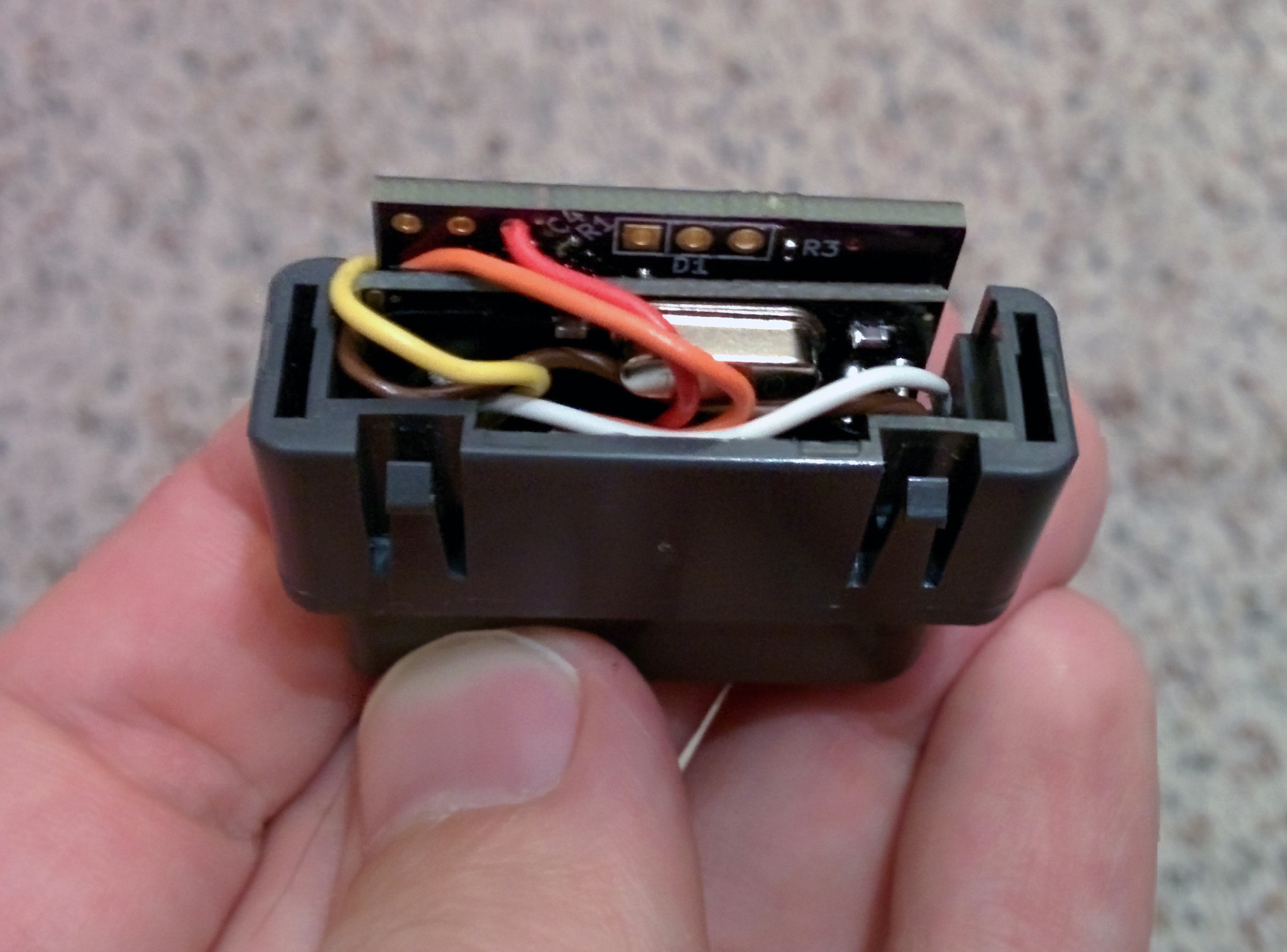
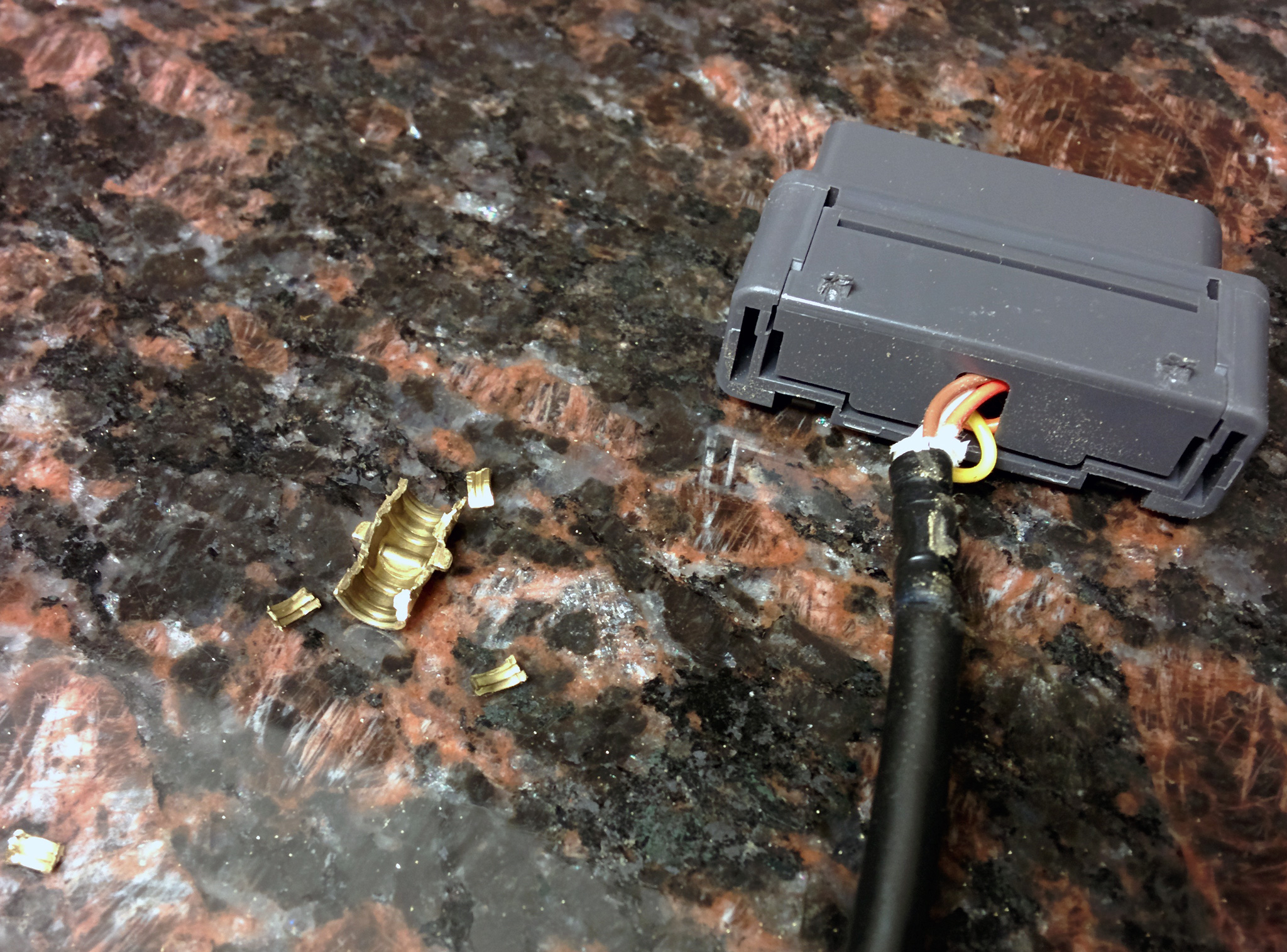
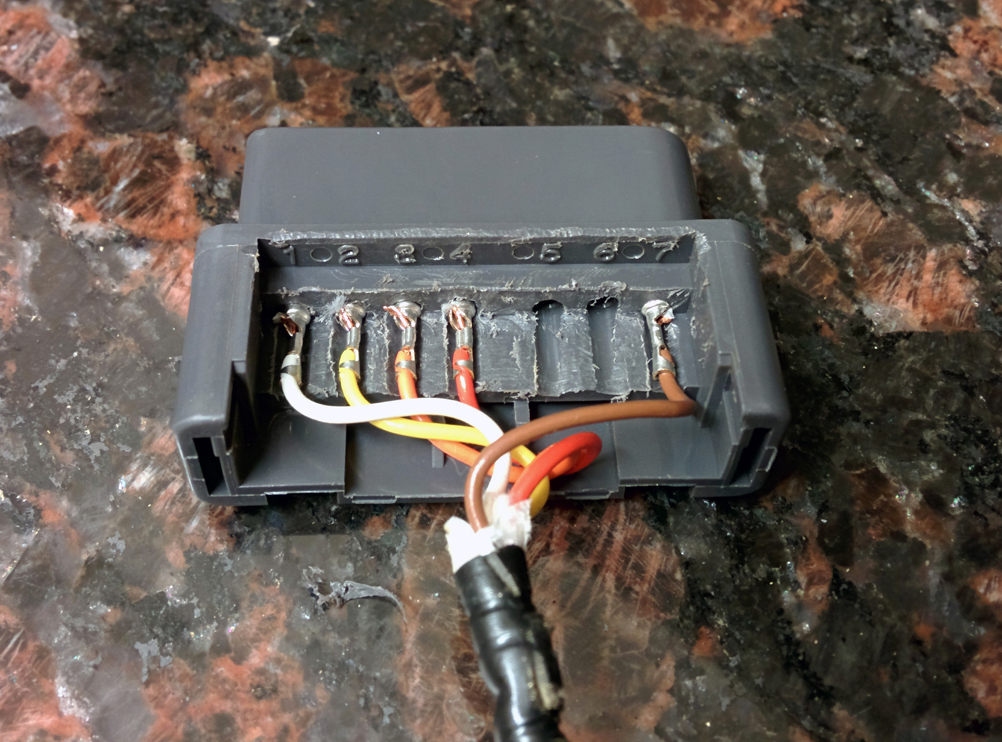
So here's the first "fully working" part! I forgot about the pins on the RF daughter board (bottom left of the first image), so they got dremeled down to fit only afterwards. And three of the wires awkwardly snaked around the edges because they were attached second, but should have been first. But it fits and works! Almost... It turns out that using super glue to affix the pins was a bad idea. In this first unit they don't quite line up correctly anymore, so I can't actually put this connector into the port on the console. I've assembled a second working one, by connecting all the pins into the port before gluing. This works, but it's very difficult to insert/remove the connector. So I plan to do a third with just hot glue, which is a bit flexible. I hope that will hold everything together enough, but be just pliable enough to allow the pins to shift into place as they mate with the connector port.
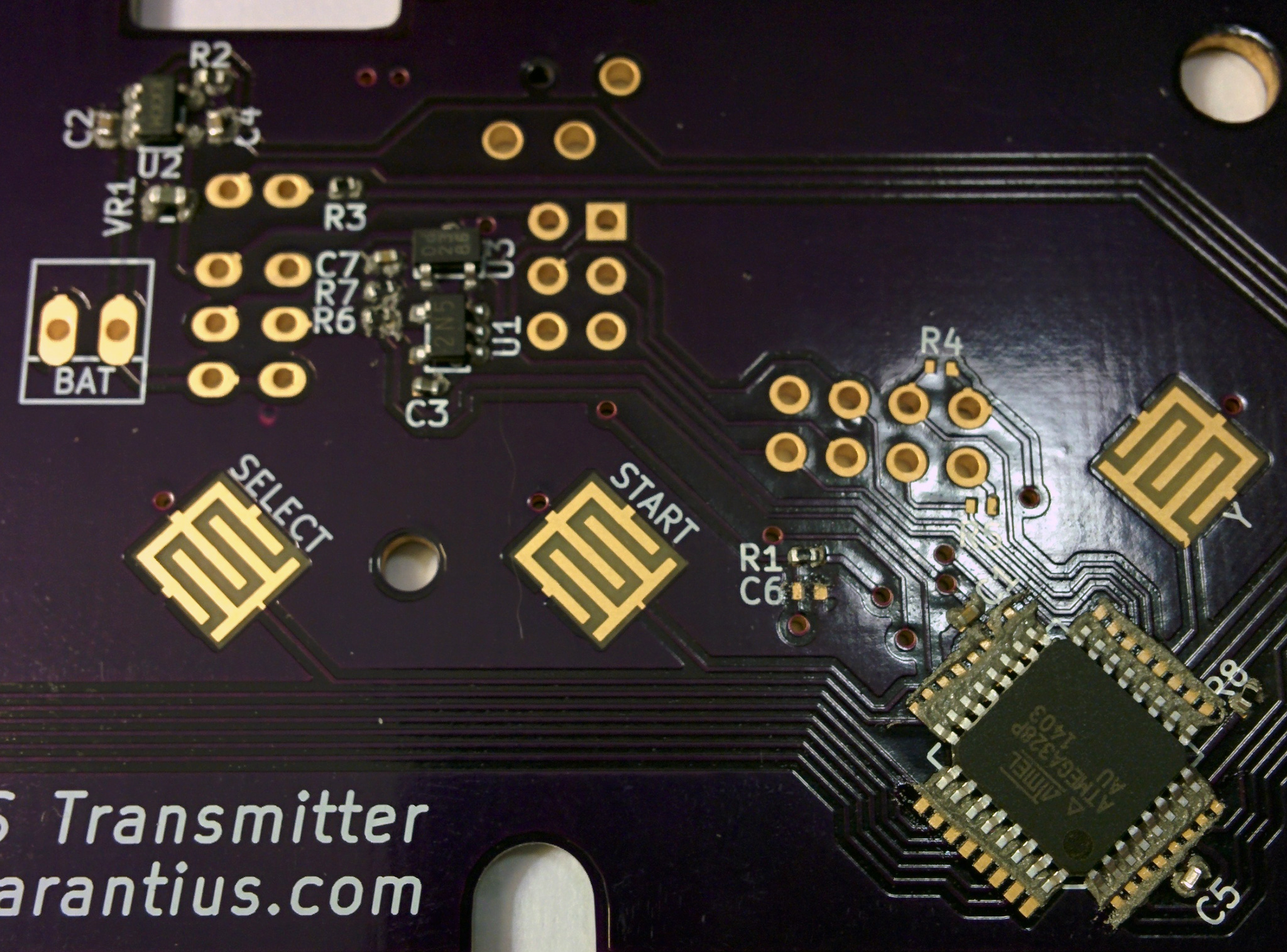
I used the breadboard transmitter circuit to test the receiver above. Once it was working, time to get a real controller assembled! Pictures above are first the board with solder paste and components attached. Note that I manually wiped off a bit of the solder paste around the microcontroller, in an attempt to avoid having it bridge the pins like before. It helped a bit, but not enough. In the process of heating the thing to melt the solder, one of the tiny surface mount resistors wasn't quite positioned properly and required manual attention. I had a devil of a time re-attaching it by hand later. You can see tiny bits of solder spread out around it as I repeatedly tried to attach it down with the iron. But I did (barely) get it lined up and soldered down. It happens to be the resistor which controls the current that the charging IC (right next to it) will apply to the battery, affecting charging time.
And with mention of the battery: I've been doing a battery test for days now! I've had the controller on, and been watching it, for nearly all my waking hours since Thursday. It took until last night (Saturday) to finally run through the whole battery. So it's got at least 24 hours of operating life on the battery, which is much better than I even hoped for. Right now I'm leaving it switched on, with a "dead" battery, to observe exactly how it behaves there. It can be unsafe to attempt to re-charge a Lithium Ion battery after discharging it too far. So I've got a chip in there to make sure that I won't over discharge it. So far signs are very good!


Here's one final note worth making. I was quite careful with everything I did here, to try to avoid waste. I didn't want to design the board, pay to have it fabricated, and only then discover a critical problem. I was almost completely successful in this regard. I missed just one physical layout issue. An earlier post showed the plastic laser cut prototype that I used to avoid this. What I failed to do was ever insert the shoulder buttons. They pivot through one of the plastic standoffs which, whoops, I blocked with my PCB. The PCB had no traces or parts there, so I could dremel it out without issue. But one of them was also blocked by the RF daughter board! By extreme luck, only a tiny bit of the corner next to, rather than part of, the antenna was actually located there. In these pictures you can see the bits that I had to chop out. Good thing I didn't need to pay another $50 to re-spin another board!
So what I've got now is one each transmitter and receiver circuit, working and tested end to end. Wonderful! What remains is to actually complete the original target of the project and hook this up to a Nintendo, not a Super Nintendo. Early in my research I discovered that they're nearly identical. So I can, if I choose, build a receiver only for the Nintendo and use the Super Nintendo controller with it. That's next. I got a cheap NES Satellite receiver only via eBay. It works via infrared, but is a nice pretty container to hold a replacement radio based unit, and I certainly won't run into any connector modification issues like before!
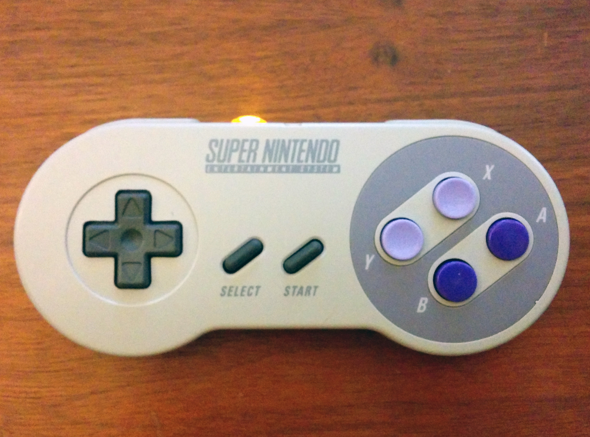
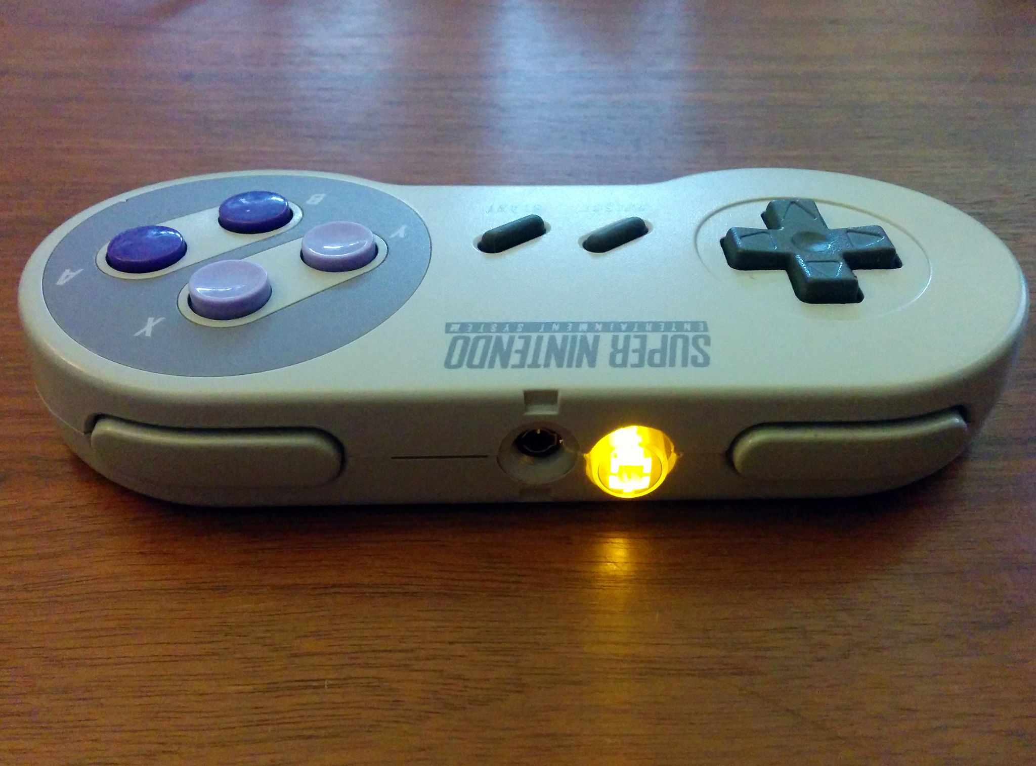
Finally, here's a picture of the final modified controller! Overall it still looks very pretty. There's a bit of a gap around the indicator/power button. The cable hole is replaced with a connector for recharging the battery. Hopefully my second controller will look even better without the gaps! I've pushed all the source to GitHub today. The hardware was designed with KiCad and the software through the Arduino IDE, with the RF24 library.